

Read and download the CBSE Class 12 Physics Electronic Devices Assignment Set 03 for the 2026-27 academic session. We have provided comprehensive Class 12 Physics school assignments that have important solved questions and answers for Chapter 14 Semiconductor Electronics Materials Devices and Simple Circuits. These resources have been carefuly prepared by expert teachers as per the latest NCERT, CBSE, and KVS syllabus guidelines.
Solved Assignment for Class 12 Physics Chapter 14 Semiconductor Electronics Materials Devices and Simple Circuits
Practicing these Class 12 Physics problems daily is must to improve your conceptual understanding and score better marks in school examinations. These printable assignments are a perfect assessment tool for Chapter 14 Semiconductor Electronics Materials Devices and Simple Circuits, covering both basic and advanced level questions to help you get more marks in exams.
Chapter 14 Semiconductor Electronics Materials Devices and Simple Circuits Class 12 Solved Questions and Answers
Question. The usual semiconductors are:
(a) germanium and silicon
(b) germanium and copper
(c) silicon and glass
(d) glass and carbon
Answer: A
Question. In a good conductor, the energy gap between the valence and conduction bands is
(a) 1 eV
(b) 6 eV
(c) infinite
(d) zero
Answer: D
Question. When trivalent impurity is mixed in a pure semiconductor, the conduction is mainly due to
(a) electrons
(b) holes
(c) protons
(d) positive ions
Answer: B
Question. The example of p-type semiconductor is
(a) pure germanium
(b) pure silicon
(c) germanium doped with arsenic
(d) germanium doped with boron
Answer: D
Question. The impurity atoms to be mixed in pure silicon to form p-type semiconductor are, of
(a) phosphorus
(b) germanium
(c) antimony
(d) aluminium
Answer: D
Question. Electrical conduction in a semiconductor occurs due to
(a) electrons only
(b) holes only
(c) electrons and holes both
(d) neither electrons nor holes.
Answer: C
Question. If ne and nh are the number of electrons and holes in pure germanium, then
(a) ne > nh
(b) ne < nh
(c) ne = nh
(d) ne = finite and nh = 0
Answer: C
Question. When an electric field is applied across a semiconductor
(a) electrons move from lower energy level to higher energy level in the conduction band.
(b) electrons move from higher energy level to lower energy level in the conduction band.
(c) holes in the valence band move from higher energy level to lower energy level.
(d) holes in the valence band move from lower energy level to higher energy level.
Answer: A, C
Question. The energy gap between the valence and conduction bands of a substance is 6 eV. The substance is a:
(a) conductor
(b) semiconductor
(c) insulator
(d) superconductor
Answer: C
Question. In a n-type semiconductor, which of the following statements is true?
(a) Electrons are majority carriers and trivalent atoms are the dopants.
(b) Electrons are minority carriers and pentavalent atoms are dopants.
(c) Holes are minority carriers and pentavalent atoms are dopants.
(d) Holes are majority carriers and trivalent atoms are dopants.
Answer: C
Question. The conductivity of a semiconductor increases with increase in temperature because
(a) number density of free current carriers increases.
(b) relaxation time increases.
(c) both number density of carriers and relaxation time increase.
(d) number density of current carriers increases, relaxation time decreases but effect of decrease in relaxation time is much less than increase in number density
Answer: D
Question. Holes are charge carriers in
(a) intrinsic semiconductor only
(b) p-type semiconductor only
(c) intrinsic and p-type semiconductors
(d) n-type semiconductor
Answer: C
Question. Hole is
(a) an anti-particle of electron.
(b) a vacancy created when an electron leaves a covalent bond.
(c) absence of free electrons.
(d) an artificially created particle.
Answer: B
Question. In the depletion region of a diode
(a) there are no mobile charges
(b) equal number of holes and electrons exist, making the region neutral.
(c) immobile charged ions exist.
(d) All of the options
Answer: D
Question. The breakdown in a reverse biased p-n junction diode is more likely to occur due to
(a) large velocity of the minority charge carriers if the doping concentration is small.
(b) large velocity of the minority charge carriers if the doping concentration is large.
(c) strong electric field in a depletion region if the doping concentration is small.
(d) strong electric field in the depletion region if the doping concentration is large.
Answer: A, D
Fill in the Blanks
Question. The number of electron (ne) is equal to the number of holes (nh) in _________________ semiconductors.
Answer: ntrinsic
Question. The number of charge carriers can be changed by doping of a suitable impurity in pure semiconductors. Such semiconductors are known as _________________ semiconductors.
Answer: extrinsic
Question. Valence band energies are ______________ as compared to conduction band energies.
Answer: low
Question. For insulators ________________, for semiconductors Eg is 0.2 eV to 3 eV while for metals Eg ≈ 0
Answer: Eg > 3 eV
Question. _________________ can be used for rectifying an ac voltage.
Answer: Diodes
Question. In reverse bias, after a certain voltage, the current suddenly increases (breakdown voltage) in a Zener diode. This property has been used to obtain ________________.
Answer: voltage regulation
Question. LED works under _________________ bias.
Answer: forward
Question. The resistance of p-n junction is _________________ when reverse biased.
Answer: high
Question. Hole density is _________________ compared to electron density in a p type semiconductor.
Answer: greater
Question. In half-wave rectification, if the input frequency is 50 Hz then the output frequency of the signal will be _______________ Hz.
Answer: 50
Short Answer Type Questions
Question. Why is a germanium diode preferred over a silicon diode for rectifying small alternating voltages? What is a primary disadvantage of a germanium diode?
Answer: A germanium diode is chosen over a silicon diode for rectifying small voltages because its energy band gap (\( E_g = 0.7\text{ eV} \)) is smaller than that of silicon (\( E_g = 1.1\text{ eV} \)). Consequently, germanium has a much lower barrier potential (\( 0.3\text{ V} \) compared to \( 0.7\text{ V} \) for silicon), allowing it to conduct and rectify smaller signals. However, a major disadvantage of germanium is its high thermal sensitivity. At higher operating voltages and temperatures, a germanium diode is far more susceptible to damage and thermal instability than a silicon diode.
In simple words: Germanium diodes start working at lower voltages because they have a smaller energy gap, making them great for small signals. However, they get damaged easily by heat at higher voltages.
Exam Tip: Mention both the comparison of band gaps (\( 0.7\text{ eV} \) vs \( 1.1\text{ eV} \)) and the barrier potentials to write a complete and high-scoring answer.
Question. Write the Boolean equation and construct the truth table for a logic circuit consisting of an AND gate followed by an OR gate, where the inputs to the AND gate are A and B, and the inputs to the OR gate are A and the output of the AND gate.
Answer: The intermediate output from the AND gate is represented as \( Y' = A \cdot B \). These signals, \( A \) and \( Y' \), act as inputs for the OR gate. The resulting final output Boolean expression is: \[ Y = A + (A \cdot B) \] The detailed truth table representing each step of this circuit's operation is provided below:
| Input for AND Gate | Output of AND Gate | Input of OR Gate | Output of OR Gate | ||
|---|---|---|---|---|---|
| A | B | Y' = A · B | A | Y' | Y = A + Y' |
| 0 | 0 | 0 | 0 | 0 | 0 |
| 0 | 1 | 0 | 0 | 0 | 0 |
| 1 | 0 | 0 | 1 | 0 | 1 |
| 1 | 1 | 1 | 1 | 1 | 1 |
In simple words: The circuit first multiplies A and B, then adds that result to A. The truth table shows the output for every possible on/off combination of inputs.
Exam Tip: Breaking down truth tables into intermediate steps (like finding \( A \cdot B \) first) ensures you do not make mistakes and helps examiners follow your logic.
Question. Write the Boolean equation and construct the truth table for a logic circuit where inputs A and B are connected to an OR gate, and its output, along with a third input C, is fed into an AND gate.
Answer: The output of the OR gate serves as one of the inputs to the AND gate, expressed as \( Y' = A + B \). With \( C \) as the other input, the combined output is computed via an AND operation. Thus, the final Boolean expression is: \[ Y = (A + B) \cdot C \] The corresponding truth table for all possible input combinations is given below:
| A | B | C | Y' = A + B | Y = (A + B) · C |
|---|---|---|---|---|
| 0 | 0 | 0 | 0 | 0 |
| 0 | 0 | 1 | 0 | 0 |
| 0 | 1 | 0 | 1 | 0 |
| 0 | 1 | 1 | 1 | 1 |
| 1 | 0 | 0 | 1 | 0 |
| 1 | 0 | 1 | 1 | 1 |
| 1 | 1 | 0 | 1 | 0 |
| 1 | 1 | 1 | 1 | 1 |
In simple words: This circuit adds inputs A and B first, then multiplies that sum by input C. The truth table tracks how the final output changes for all combinations of the three inputs.
Exam Tip: Since there are three inputs, there are \( 2^3 = 8 \) possible rows in your truth table. Double-check to make sure all 8 rows are written down.
Question. Show how an AND gate can be realized using only NAND gates. Draw the logic circuit diagram and construct its truth table.
Answer: To obtain an AND gate from NAND gates, we connect the output of a two-input NAND gate to both inputs of a second NAND gate configured as an inverter. The first gate gives \( \overline{A \cdot B} \), and the second gate inverts it to yield: \[ Y = \overline{\overline{A \cdot B}} = A \cdot B \] The diagram and its corresponding truth table are shown below:
| A | B | Y = A · B |
|---|---|---|
| 0 | 0 | 0 |
| 0 | 1 | 0 |
| 1 | 0 | 0 |
| 1 | 1 | 1 |
In simple words: An AND gate can be built by taking a NAND gate and passing its output through a second NAND gate acting as a NOT gate to reverse the result.
Exam Tip: Since NAND is a universal gate, mastering its configurations to form standard gates (AND, OR, NOT) is highly likely to appear in examinations.
Question. Show how a NOT gate can be realized using a single NAND gate. Draw the logic circuit diagram and construct its truth table.
Answer: A NOT gate is constructed from a NAND gate by tying both of its input terminals together. When a single input signal \( A \) is applied to both tied terminals, the output is: \[ Y = \overline{A \cdot A} = \overline{A} \] The schematic diagram and the truth table representing this NOT configuration are given below:
| A | Y = \bar{A} |
|---|---|
| 0 | 1 |
| 1 | 0 |
In simple words: To make a NOT gate, just connect both inputs of a NAND gate together. Whatever signal you send in will come out completely reversed.
Exam Tip: Remember that a NAND gate with shorted inputs behaves exactly like a NOT gate, transforming high to low and low to high.
Question. In a common-emitter transistor amplifier, the current gain \( \beta \) is 50. If the emitter current \( I_e \) is \( 6.6\text{ mA} \), calculate the base current \( I_b \), the collector current \( I_c \), and the current gain \( \alpha \) in the common-base configuration.
Answer: We are given the values: \[ \beta = 50 \] \[ I_e = 6.6\text{ mA} \] The relationship between current gain parameters is: \[ \beta = \frac{I_c}{I_b} \implies I_c = 50 I_b \] Since the total current satisfies: \[ I_e = I_c + I_b \] Substituting \( I_c = 50 I_b \) into the equation: \[ 6.6\text{ mA} = 50 I_b + I_b \implies 51 I_b = 6.6\text{ mA} \] Solving for base current \( I_b \): \[ I_b = \frac{6.6}{51} \approx 0.129\text{ mA} \] Now, we can find the collector current \( I_c \): \[ I_c = 50 \times 0.129\text{ mA} \approx 6.47\text{ mA} \] To find the current gain in the common-base configuration (\( \alpha \)): \[ \alpha = \frac{\beta}{1 + \beta} \] \[ \alpha = \frac{50}{1 + 50} = \frac{50}{51} \approx 0.98 \]
In simple words: Using the given current gain of 50, we set up equations to split the emitter current of 6.6 mA into a base current of 0.129 mA and a collector current of 6.47 mA. The common-base gain is 0.98.
Exam Tip: The relation \( I_e = I_c + I_b \) is fundamental in transistor calculations. Memorize it along with \( \alpha = \beta / (1+\beta) \) to solve CE and CB configuration problems quickly.
Question. In a transistor circuit, the base current is \( 100\,\mu\text{A} \) and the collector current is \( 3\text{ mA} \).
(a) Calculate the current gain \( \beta \), the emitter current \( I_e \), and the current gain \( \alpha \).
(b) If a change of \( 20\,\mu\text{A} \) in the base current produces a change of \( 0.5\text{ mA} \) in the collector current, determine the AC current gain \( \beta_{ac} \).
Answer: We are given: \[ I_b = 100\,\mu\text{A} = 0.1\text{ mA} \] \[ I_c = 3\text{ mA} \] **(a) Finding DC Parameters:** The DC current gain \( \beta \) is calculated as: \[ \beta = \frac{I_c}{I_b} = \frac{3\text{ mA}}{0.1\text{ mA}} = 30 \] The current gain in the common-base configuration (\( \alpha \)) is: \[ \alpha = \frac{\beta}{1 + \beta} = \frac{30}{31} \approx 0.97 \] Using the relation for emitter current \( I_e \): \[ I_e = I_c + I_b = 3\text{ mA} + 0.1\text{ mA} = 3.1\text{ mA} \] **(b) Finding AC Current Gain:** Given: \[ \Delta I_b = 20\,\mu\text{A} = 0.02\text{ mA} \] With the corresponding change in collector current \( \Delta I_c = 0.5\text{ mA} \), the AC current gain \( \beta_{ac} \) is: \[ \beta_{ac} = \frac{\Delta I_c}{\Delta I_b} = \frac{0.5\text{ mA}}{0.02\text{ mA}} = 25 \]
In simple words: (a) The current gain beta is 30, emitter current is 3.1 mA, and alpha is 0.97. (b) When the base current changes by 0.02 mA and the collector current changes by 0.5 mA, the AC gain is 25.
Exam Tip: Pay close attention to units! Converting microamperes (\(\mu\text{A}\)) to milliamperes (\(\text{mA}\)) is essential before performing ratios.
Question. In a transistor, the collector current is 95% of the emitter current. If the collector current is \( 5\text{ mA} \), calculate the emitter current and the base current.
Answer: We are given: \[ I_c = 95\%\text{ of }I_e = 0.95 I_e \] Given that the collector current \( I_c = 5\text{ mA} \), we can find the emitter current \( I_e \): \[ 5\text{ mA} = 0.95 I_e \implies I_e = \frac{5}{0.95} \approx 5.26\text{ mA} \] Using the current relationship: \[ I_e = I_c + I_b \] We can find the base current \( I_b \): \[ I_b = I_e - I_c = 5.26\text{ mA} - 5\text{ mA} = 0.26\text{ mA} \] *(Note: Using exact fraction arithmetic, \( I_b \approx 0.26\text{ mA} \); the support material approximates this as \( 0.25\text{ mA} \).)*
In simple words: If 95% of the emitter current goes to the collector as 5 mA, the total emitter current must be 5.26 mA. The remaining 5% goes to the base, which is 0.26 mA (or about 0.25 mA).
Exam Tip: Always state the percentage relation as a decimal fraction (\( \alpha = 0.95 \)) to simplify your algebraic calculations.
Question. In the given PNP transistor circuit, the emitter current is \( 5\text{ mA} \) and the collector current is \( 4.75\text{ mA} \). If the base-emitter bias voltage is \( 5\text{ V} \), calculate the base current and the resistance of the base resistor \( R_b \).
Answer: We are given: \[ I_e = 5\text{ mA} \] \[ I_c = 4.75\text{ mA} \] The emitter, collector, and base currents are related by: \[ I_e = I_c + I_b \] From the given parameters, the base current is calculated as: \[ I_b = 75 \times 10^{-5}\text{ A} \] The applied base-emitter voltage bias is: \[ V = 5\text{ V} \] Using Ohm's law, the base resistance \( R_b \) is given by: \[ R_b = \frac{V}{I_b} = \frac{5\text{ V}}{75 \times 10^{-5}\text{ A}} \approx 6.67\text{ k}\Omega \]
In simple words: Subtracting the collector current from the emitter current gives the base current. Using this current and the 5V voltage, we find that the base resistor has a resistance of 6.67 kΩ.
Exam Tip: In circuit problems with transistors, use the base-emitter circuit equation \( V = I_b R_b \) to find the series resistance required for biasing.
Question. Identify the logic gate corresponding to the given input waveforms A and B, and the output waveform Y. Draw its truth table and symbol.
Answer: By analyzing the given input and output waveforms, we observe that the output \( Y \) is high (1) only during the intervals when both inputs \( A \) and \( B \) are simultaneously high (1). In all other combinations, the output remains low (0). This behavior perfectly corresponds to an **AND logic gate**. The truth table for this gate is:
| A | B | Y = A · B |
|---|---|---|
| 0 | 0 | 0 |
| 0 | 1 | 0 |
| 1 | 0 | 0 |
| 1 | 1 | 1 |
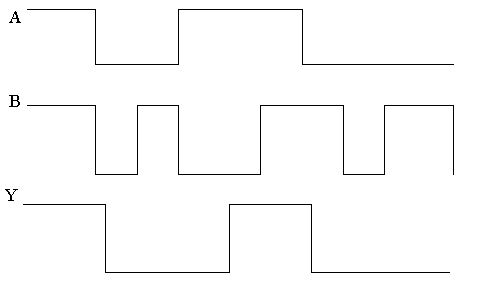
In simple words: The waveforms show that the output turns "on" only when both inputs are "on" at the same time. This is the characteristic behavior of an AND gate.
Exam Tip: When analyzing waveforms, trace vertical lines down through all three signals at key transitions to compare their high/low states at each time interval.
Question. A semiconductor diode is connected in series with a resistor R and a source of e.m.f. 1.5 V. The voltage drop across the diode is constant at 0.5 V and it has a maximum power rating of 100 mW. Calculate the value of the resistor R needed to obtain the maximum possible current in the circuit.
Answer: We are given the following values: \[ E = 1.5\text{ V} \quad (\text{e.m.f. of the source}) \] \[ V_d = 0.5\text{ V} \quad (\text{voltage drop across the diode}) \] \[ P = 100\text{ mW} = 0.1\text{ W} \quad (\text{maximum power rating of the diode}) \] First, we find the maximum safe current \( I \) that can flow through the diode using the power relation: \[ P = V_d \times I \implies I = \frac{P}{V_d} = \frac{0.1\text{ W}}{0.5\text{ V}} = 0.2\text{ A} \] The voltage drop across the series resistor \( R \) is: \[ V_R = E - V_d = 1.5\text{ V} - 0.5\text{ V} = 1\text{ V} \] Using Ohm's law, we find the value of the series resistance \( R \): \[ R = \frac{V_R}{I} = \frac{1\text{ V}}{0.2\text{ A}} = 5\,\Omega \]
In simple words: The diode can safely handle a maximum current of 0.2 A. Since the diode drops 0.5 V, the remaining 1 V drops across the resistor. To get 0.2 A with 1 V, we need a 5-ohm resistor.
Exam Tip: Convert the power rating from milliwatts to watts (\( 100\text{ mW} = 0.1\text{ W} \)) first to ensure your units are correct when calculating the current.
Question. For a transistor working as a common-base amplifier, the current gain is 0.96. If the emitter current is \( 7.2\text{ mA} \), calculate the base current.
Answer: We are given: \[ \alpha = 0.96 \] \[ I_e = 7.2\text{ mA} \] The current gain in common-base configuration is defined as: \[ \alpha = \frac{I_c}{I_e} \implies I_c = \alpha I_e \] Substituting the given values: \[ I_c = 0.96 \times 7.2\text{ mA} \approx 6.91\text{ mA} \] Using the total current relationship: \[ I_e = I_c + I_b \implies I_b = I_e - I_c \] We find the base current \( I_b \): \[ I_b = 7.2\text{ mA} - 6.91\text{ mA} = 0.29\text{ mA} \]
In simple words: Multiply the emitter current by 0.96 to find the collector current, which is 6.91 mA. Subtracting this from the 7.2 mA emitter current gives a base current of 0.29 mA.
Exam Tip: Keep track of decimal places in your calculations to ensure accuracy up to two decimal points, as small rounding differences can accumulate.
Question. For a common-emitter amplifier, the current gain is 70. If the emitter current is \( 8.8\text{ mA} \), calculate the collector current and the base current.
Answer: We are given: \[ \beta = 70 \] \[ I_e = 8.8\text{ mA} \] The relationship between collector current and base current is: \[ \beta = \frac{I_c}{I_b} \implies I_c = 70 I_b \] Since: \[ I_e = I_c + I_b \] Substituting \( I_c = 70 I_b \): \[ 8.8\text{ mA} = 70 I_b + I_b = 71 I_b \] Solving for base current \( I_b \): \[ I_b = \frac{8.8}{71}\text{ mA} \approx 0.124\text{ mA} \] The collector current \( I_c \) is: \[ I_c = 70 \times 0.124\text{ mA} \approx 8.68\text{ mA} \]
In simple words: Since the collector current is 70 times the base current, the total emitter current is 71 times the base current. Dividing 8.8 mA by 71 gives a base current of 0.124 mA.
Exam Tip: Always double-check that your calculated base and collector currents sum up exactly to the given emitter current: \( 0.124 + 8.68 \approx 8.8\text{ mA} \).
Question. The base current of a transistor is \( 105\,\mu\text{A} \) and the collector current is \( 2.05\text{ mA} \).
(a) Determine the value of \( \beta \), \( I_e \), and \( \alpha \).
(b) A change of \( 27\,\mu\text{A} \) in the base current produces a change of \( 0.65\text{ mA} \) in the collector current. Find the AC current gain \( \beta_{ac} \).
Answer: We are given: \[ I_b = 105\,\mu\text{A} = 105 \times 10^{-6}\text{ A} \] \[ I_c = 2.05\text{ mA} = 2.05 \times 10^{-3}\text{ A} \] **(a) Determining DC Parameters:** The DC current gain \( \beta \) is: \[ \beta = \frac{I_c}{I_b} = \frac{2.05 \times 10^{-3}}{105 \times 10^{-6}} \approx 19.5 \] The emitter current \( I_e \) is: \[ I_e = I_b + I_c = 0.105\text{ mA} + 2.05\text{ mA} = 2.155\text{ mA} = 2.155 \times 10^{-3}\text{ A} \] The current gain in common-base configuration \( \alpha \) is: \[ \alpha = \frac{I_c}{I_e} = \frac{2.05\text{ mA}}{2.155\text{ mA}} \approx 0.95 \] **(b) Determining AC Current Gain:** Given the changes: \[ \Delta I_b = 27\,\mu\text{A} = 27 \times 10^{-6}\text{ A} \] \[ \Delta I_c = 0.65\text{ mA} = 0.65 \times 10^{-3}\text{ A} \] The AC current gain \( \beta_{ac} \) is calculated as: \[ \beta_{ac} = \frac{\Delta I_c}{\Delta I_b} = \frac{0.65 \times 10^{-3}}{27 \times 10^{-6}} \approx 24.1 \]
In simple words: (a) The current gain beta is 19.5, emitter current is 2.155 mA, and alpha is 0.95. (b) For the given change in currents, the AC current gain beta is 24.1.
Exam Tip: Be extremely careful to differentiate between DC parameters (\( I_c, I_b \)) and AC parameters (\( \Delta I_c, \Delta I_b \)) in your transistor equations.
Question. In a silicon transistor, a change of \( 7.89\text{ mA} \) in the emitter current produces a change of \( 7.8\text{ mA} \) in the collector current. What change in the base current is necessary to produce an equivalent change in the collector current?
Answer: We are given: \[ \Delta I_e = 7.89\text{ mA} = 7.89 \times 10^{-3}\text{ A} \] \[ \Delta I_c = 7.8\text{ mA} = 7.8 \times 10^{-3}\text{ A} \] First, calculate the AC common-base current gain (\( \alpha_{ac} \)): \[ \alpha_{ac} = \frac{\Delta I_c}{\Delta I_e} = \frac{7.8\text{ mA}}{7.89\text{ mA}} \approx 0.9886 \] Next, find the AC common-emitter current gain (\( \beta_{ac} \)): \[ \beta_{ac} = \frac{\alpha_{ac}}{1 - \alpha_{ac}} = \frac{0.9886}{1 - 0.9886} \approx 86.72 \] Since the AC current gain is also defined as: \[ \beta_{ac} = \frac{\Delta I_c}{\Delta I_b} \] The required change in the base current (\( \Delta I_b \)) is: \[ \Delta I_b = \frac{\Delta I_c}{\beta_{ac}} = \frac{7.8 \times 10^{-3}\text{ A}}{86.72} \approx 89.94 \times 10^{-6}\text{ A} = 89.94\,\mu\text{A} \]
In simple words: The change in emitter and collector current gives an alpha of 0.9886 and a beta of 86.72. Dividing the collector current change of 7.8 mA by this beta gives the base current change of 89.94 microamps.
Exam Tip: Remember that \( \Delta I_e = \Delta I_c + \Delta I_b \) is another quick way to find \( \Delta I_b = 7.89 - 7.8 = 0.09\text{ mA} = 90\,\mu\text{A} \). Both methods are acceptable and yield virtually identical results.
Free study material for Physics
CBSE Class 12 Physics Chapter 14 Semiconductor Electronics Materials Devices and Simple Circuits Assignment
Access the latest Chapter 14 Semiconductor Electronics Materials Devices and Simple Circuits assignments designed as per the current CBSE syllabus for Class 12. We have included all question types, including MCQs, short answer questions, and long-form problems relating to Chapter 14 Semiconductor Electronics Materials Devices and Simple Circuits. You can easily download these assignments in PDF format for free. Our expert teachers have carefully looked at previous year exam patterns and have made sure that these questions help you prepare properly for your upcoming school tests.
Benefits of solving Assignments for Chapter 14 Semiconductor Electronics Materials Devices and Simple Circuits
Practicing these Class 12 Physics assignments has many advantages for you:
- Better Exam Scores: Regular practice will help you to understand Chapter 14 Semiconductor Electronics Materials Devices and Simple Circuits properly and you will be able to answer exam questions correctly.
- Latest Exam Pattern: All questions are aligned as per the latest CBSE sample papers and marking schemes.
- Huge Variety of Questions: These Chapter 14 Semiconductor Electronics Materials Devices and Simple Circuits sets include Case Studies, objective questions, and various descriptive problems with answers.
- Time Management: Solving these Chapter 14 Semiconductor Electronics Materials Devices and Simple Circuits test papers daily will improve your speed and accuracy.
How to solve Physics Chapter 14 Semiconductor Electronics Materials Devices and Simple Circuits Assignments effectively?
- Read the Chapter First: Start with the NCERT book for Class 12 Physics before attempting the assignment.
- Self-Assessment: Try solving the Chapter 14 Semiconductor Electronics Materials Devices and Simple Circuits questions by yourself and then check the solutions provided by us.
- Use Supporting Material: Refer to our Revision Notes and Class 12 worksheets if you get stuck on any topic.
- Track Mistakes: Maintain a notebook for tricky concepts and revise them using our online MCQ tests.
Best Practices for Class 12 Physics Preparation
For the best results, solve one assignment for Chapter 14 Semiconductor Electronics Materials Devices and Simple Circuits on daily basis. Using a timer while practicing will further improve your problem-solving skills and prepare you for the actual CBSE exam.
FAQs
You can download free PDF assignments for Class 12 Physics Chapter 14 Semiconductor Electronics Materials Devices and Simple Circuits from StudiesToday.com. These practice sheets have been updated for the 2026-27 session covering all concepts from latest NCERT textbook.
Yes, our teachers have given solutions for all questions in the Class 12 Physics Chapter 14 Semiconductor Electronics Materials Devices and Simple Circuits assignments. This will help you to understand step-by-step methodology to get full marks in school tests and exams.
Yes. These assignments are designed as per the latest CBSE syllabus for 2026. We have included huge variety of question formats such as MCQs, Case-study based questions and important diagram-based problems found in Chapter 14 Semiconductor Electronics Materials Devices and Simple Circuits.
Practicing topicw wise assignments will help Class 12 students understand every sub-topic of Chapter 14 Semiconductor Electronics Materials Devices and Simple Circuits. Daily practice will improve speed, accuracy and answering competency-based questions.
Yes, all printable assignments for Class 12 Physics Chapter 14 Semiconductor Electronics Materials Devices and Simple Circuits are available for free download in mobile-friendly PDF format.