
Read and download free pdf of CBSE Class 12 Physics Semiconductor Materials Device And Simple Worksheet. Download printable Physics Class 12 Worksheets in pdf format, CBSE Class 12 Physics Chapter 14 Semiconductor Electronics Materials Devices and Simple Circuits Worksheet has been prepared as per the latest syllabus and exam pattern issued by CBSE, NCERT and KVS. Also download free pdf Physics Class 12 Assignments and practice them daily to get better marks in tests and exams for Class 12. Free chapter wise worksheets with answers have been designed by Class 12 teachers as per latest examination pattern
Chapter 14 Semiconductor Electronics Materials Devices and Simple Circuits Physics Worksheet for Class 12
Class 12 Physics students should refer to the following printable worksheet in Pdf in Class 12. This test paper with questions and solutions for Class 12 Physics will be very useful for tests and exams and help you to score better marks
Class 12 Physics Chapter 14 Semiconductor Electronics Materials Devices and Simple Circuits Worksheet Pdf
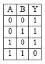
Question. In the following circuit, the output Y for all possible inputs A and B is expressed by the truth table.
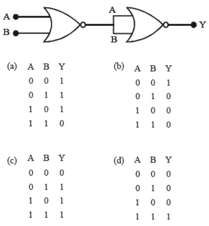
Answer: C
Question. What is the voltage gain in a common emitter amplifier, where input resistance is 3 Ω and load resistance 24 Ω, β = 0.6 ?
(a) 8 . 4
(b) 4 . 8
(c) 2 . 4
(d) 480
Answer: B
Question. In a common emitter transistor amplifier β = 60, Ro = 5000 Ω and internal resistance of a transistor is 500 Ω. The voltage amplification of amplifier will be
(a) 500
(b) 460
(c) 600
(d) 560
Answer: C
Question. The band gap in germanium and silicon in ev respectively is
(a) 1.1, 0
(b) 0, 1.1
(c) 1.1, 0.7
(d) 0.7, 1.1
Answer: D
Question. A transistor has three impurity regions. All the three regions have different doping levels. In order of increasing doping level, the regions are
(a) emitter, base and collector
(b) collector, base and emitter
(c) base, emitter and collector
(d) base, collector and emitter
Answer: D
Question. In a common base amplifier the phase difference between the input signal voltage and the output voltage is
(a) 0
(b) π/4
(c) π/2
(d) π
Answer: A
Question. The following circut represents
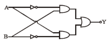
(a) OR gate
(b) XOR gate
(c) AND gate
(d) NAND gate
Answer: B
Question. The electrical conductivity of a semiconductor increases when electromagnetic radiation of wavelength shorter than 2480 nm is incident on it. The band gap (in eV) for the semiconductor is
(a) 0.9
(b) 0.7
(c) 0.5
(d) 1.1
Answer: C
Question. The diagram of a logic circuit is given below. The output F of the circuit is represented by
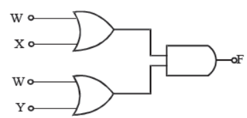
(a) W . (X + Y)
(b) W . (X . Y)
(c) W + (X . Y)
(d) W + (X + Y)
Answer: C
Question. In the half wave rectifier circuit operating from 50 Hz mains frequency, the fundamental frequency in the ripple would be
(a) 25 Hz
(b) 50 Hz
(c) 70.7 Hz
(d) 100 Hz
Answer: B
Question. A transistor is operated in common emitter configuration at VC = 2V such that a change in the base current from 100 mA to 300 mA produces a change in the collector current from 10mA to 20 mA. The current gain is
(a) 50
(b) 75
(c) 100
(d) 25
Answer: A
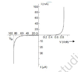
Question. In a p-n junction having depletion layer of thickness 10–6 m the potential across it is 0.1 V. The electric field is
(a) 107 V/m
(b) 10–6 V/m
(c) 105 V/m
(d) 10–5 V/m
Answer: C
Question. In the diagram, the input is across the terminals A and C and the output is across B and D. Then the output is
(a) zero
(b) same as the input
(c) full wave rectifier
(d) half wave rectifier
Answer: C
Question. A half-wave rectifier is being used to rectify an alternating voltage of frequency 50 Hz. The number of pulses of rectified current obtained in one second is
(a) 50
(b) 25
(c) 100
(d) 2000
Answer: B
Question. What is the conductivity of a semiconductor if electron density = 5 × 10¹²/cm3 and hole density = 8 × 10¹³/cm3 (μe = 2.3 m2 V–1 s–1, μh = 0.01 m2V–1 s–1)
(a) 5.634
(b) 1.968
(c) 3.421
(d) 8.964.
Answer: B
Question. The cause of the potential barrier in a p-n diode is
(a) depletion of positive charges near the junction
(b) concentration of positive charges near the junction
(c) depletion of negative charges near the junction
(d) concentration of positive and negative charges near the junction
Answer: D
Question. The ratio of electron and hole currents in a semiconductor is 7/4 and the ratio of drift velocities of electrons and holes is 5/4, then the ratio of concentrations of electrons and holes will be
(a) 5/7
(b) 7/5
(c) 25/49
(d) 49/25
Answer: B
Question. If A is the atomic mass number of an element, N is the Avogadro number and a is the lattice parameter, then the density of the element, if it has bcc crystal structure, is
(a) A/Na3
(b) 2A/Na3
(c) √3A/Na3
(d) 2√2A/Na3
Answer: B
Question. The current gain in transistor in common base mode is 0.99. To change the emitter current by 5 mA, the necessary change in collector will be
(a) 0.196 mA
(b) 2.45 mA
(c) 4.95 mA
(d) 5.1 mA
Answer: C
Question. In a reverse biased diode when the applied voltage changes by 1 V, the current is found to change by 0.5 μA. The reverse bias resistance of the diode is
(a) 2 × 10⁵ Ω
(b) 2 × 10⁶ Ω
(c) 200 Ω
(d) 2 Ω.
Answer: B
Question. The output of the given circuit in figure given below,
(a) would be zero at all times
(b) would be like a half wave rectifier with positive cycles in output
(c) would be like a half wave rectifier with negative cycles in output
(d) would be like that of a full wave rectifier
Answer: C
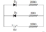
Question. In the circuit shown in figure given below, if the diode forward voltage drop is 0.3 V, the voltage difference between A and B is
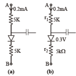
(a) 1.3 V
(b) 2.3 V
(c) 0
(d) 0.5 V
Answer: B
Question. The transistor are usually made of
(a) metal oxides with high temperature coefficient of resistivity
(b) metals with high temperature coefficient of resistivity
(c) metals with low temperature coefficient of resistivity
(d) semiconducting materials having low temperature coefficient of resistivity
Answer: A
Question. The truth table given below is for
(a) NOR
(b) AND
(c) XOR
(d) NAND
Answer: D
Question. In a full wave rectifier circuit operating from 50 Hz mains frequency, the fundamental frequency in the ripple would be
(a) 25 Hz
(b) 50 Hz
(c) 70.7 Hz
(d) 100 Hz
Answer: D
Question. The manifestation of band structure in solids is due to
(a) Bohr’s correspondence principle
(b) Pauli’s exclusion principle
(c) Heisenberg’s uncertainty principle
(d) Boltzmann’s law
Answer: B
Question. The frequency response curve of RC coupled amplifier is shown in figure. The band with of the amplifier will be (35 ex 2)
(a) f3 – f2
(b) f4 – f1
(c) f4 – f2/2
(d) f3 – f1
Answer: B
Question. A diode having potential difference 0.5 V across its junction which does not depend on current, is connected in series with resistance of 20Ω across source. If 0.1 A current passes through resistance then what is the voltage of the source?
(a) 1.5 V
(b) 2.0 V
(c) 2.5 V
(d) 5 V
Answer: C
Question. The difference in the variation of resistance with temperature in a metal and a semiconductor arises essentially due to the difference in the
(a) crystal structure
(b) variation of the number of charge carriers with temperature
(c) type of bonding
(d) variation of scattering mechanism with temperature
Answer: B
Question. Carbon, Silicon and Germanium atoms have four valence electrons each. Their valence and conduction bands are separated by energy band gaps represented by (Eg)C, (Eg)Si and (Eg)Ge respectively. Which one of the following relationship is true in their case?
(a) (Eg)C > (Eg)Si
(b) (Eg)C < (Eg)Si
(c) (Eg)C = (Eg)Si
(d) (Eg)C < (Eg)Ge
Answer: A
Please click on below link to download CBSE Class 12 Physics Semiconductor Materials Device And Simple Worksheet
| CBSE Class 12 Physics Alternating Current Worksheet Set A |
| CBSE Class 12 Physics Alternating Current Worksheet Set B |
| CBSE Class 12 Physics Electromagnetic Waves Worksheet |
| CBSE Class 12 Physics Wave Optics Worksheet |
| CBSE Class 12 Physics Wave Optics Worksheet Set A |
| CBSE Class 12 Physics Atoms And Nuclei Worksheet |
| CBSE Class 12 Physics Atoms Worksheet Set A |
| CBSE Class 12 Physics Nuclei Worksheet |
| CBSE Class 12 Physics Semiconductor Devices And Communication System Worksheet |
| CBSE Class 12 Physics Semiconductor Materials Device And Simple Worksheet |
More Study Material
CBSE Class 12 Physics Chapter 14 Semiconductor Electronics Materials Devices and Simple Circuits Worksheet
The above practice worksheet for Chapter 14 Semiconductor Electronics Materials Devices and Simple Circuits has been designed as per the current syllabus for Class 12 Physics released by CBSE. Students studying in Class 12 can easily download in Pdf format and practice the questions and answers given in the above practice worksheet for Class 12 Physics on a daily basis. All the latest practice worksheets with solutions have been developed for Physics by referring to the most important and regularly asked topics that the students should learn and practice to get better scores in their examinations. Studiestoday is the best portal for Printable Worksheets for Class 12 Physics students to get all the latest study material free of cost.
Worksheet for Physics CBSE Class 12 Chapter 14 Semiconductor Electronics Materials Devices and Simple Circuits
Teachers of studiestoday have referred to the NCERT book for Class 12 Physics to develop the Physics Class 12 worksheet. If you download the practice worksheet for the above chapter daily, you will get better scores in Class 12 exams this year as you will have stronger concepts. Daily questions practice of Physics printable worksheet and its study material will help students to have a stronger understanding of all concepts and also make them experts on all scoring topics. You can easily download and save all revision Worksheets for Class 12 Physics also from www.studiestoday.com without paying anything in Pdf format. After solving the questions given in the practice sheet which have been developed as per the latest course books also refer to the NCERT solutions for Class 12 Physics designed by our teachers
Chapter 14 Semiconductor Electronics Materials Devices and Simple Circuits worksheet Physics CBSE Class 12
All practice paper sheet given above for Class 12 Physics have been made as per the latest syllabus and books issued for the current academic year. The students of Class 12 can be assured that the answers have been also provided by our teachers for all test paper of Physics so that you are able to solve the problems and then compare your answers with the solutions provided by us. We have also provided a lot of MCQ questions for Class 12 Physics in the worksheet so that you can solve questions relating to all topics given in each chapter. All study material for Class 12 Physics students have been given on studiestoday.
Chapter 14 Semiconductor Electronics Materials Devices and Simple Circuits CBSE Class 12 Physics Worksheet
Regular printable worksheet practice helps to gain more practice in solving questions to obtain a more comprehensive understanding of Chapter 14 Semiconductor Electronics Materials Devices and Simple Circuits concepts. Practice worksheets play an important role in developing an understanding of Chapter 14 Semiconductor Electronics Materials Devices and Simple Circuits in CBSE Class 12. Students can download and save or print all the printable worksheets, assignments, and practice sheets of the above chapter in Class 12 Physics in Pdf format from studiestoday. You can print or read them online on your computer or mobile or any other device. After solving these you should also refer to Class 12 Physics MCQ Test for the same chapter.
Worksheet for CBSE Physics Class 12 Chapter 14 Semiconductor Electronics Materials Devices and Simple Circuits
CBSE Class 12 Physics best textbooks have been used for writing the problems given in the above worksheet. If you have tests coming up then you should revise all concepts relating to Chapter 14 Semiconductor Electronics Materials Devices and Simple Circuits and then take out a print of the above practice sheet and attempt all problems. We have also provided a lot of other Worksheets for Class 12 Physics which you can use to further make yourself better in Physics
You can download the CBSE Practice worksheets for Class 12 Physics Chapter 14 Semiconductor Electronics Materials Devices and Simple Circuits for the latest session from StudiesToday.com
Yes, you can click on the links above and download chapter-wise Practice worksheets in PDFs for Class 12 for Physics Chapter 14 Semiconductor Electronics Materials Devices and Simple Circuits
Yes, the Practice worksheets issued for Chapter 14 Semiconductor Electronics Materials Devices and Simple Circuits Class 12 Physics have been made available here for the latest academic session
You can easily access the links above and download the Class 12 Practice worksheets Physics for Chapter 14 Semiconductor Electronics Materials Devices and Simple Circuits
There is no charge for the Practice worksheets for Class 12 CBSE Physics Chapter 14 Semiconductor Electronics Materials Devices and Simple Circuits you can download everything free
Regular revision of practice worksheets given on studiestoday for Class 12 subject Physics Chapter 14 Semiconductor Electronics Materials Devices and Simple Circuits can help you to score better marks in exams
Yes, studiestoday.com provides all the latest Class 12 Physics Chapter 14 Semiconductor Electronics Materials Devices and Simple Circuits test practice sheets with answers based on the latest books for the current academic session
Yes, studiestoday provides worksheets in Pdf for Chapter 14 Semiconductor Electronics Materials Devices and Simple Circuits Class 12 Physics in mobile-friendly format and can be accessed on smartphones and tablets.
Yes, practice worksheets for Class 12 Physics Chapter 14 Semiconductor Electronics Materials Devices and Simple Circuits are available in multiple languages, including English, Hindi